AIM Photonics Logo


AIM Photonics — American Institute for Manufacturing Integrated Photonics

Fast Facts

Established

July 2015

Website www.aimphotonics.com

Mission Advance integrated photonic circuit manufacturing technology development while simultaneously providing access to state-of-the-art fabrication, packaging, and testing capabilities for small-to-medium enterprises, academia, and the government; create an adaptive integrated photonic circuit workforce capable of meeting industry needs and further increase domestic competitiveness; and meet participating commercial, defense, and civilian agency needs in this burgeoning technology area.

Headquarters Albany, NY (photonic chip fabrication facility)
Rochester, NY (photonic chip test, assembly, and packaging facility)

Consortium Organizer Research Foundation for the State University of New York

Satellite Locations
  • Santa Barbara, CA
  • Tucson, AZ
  • Cambridge, MA
 
   
Institute Metrics
 as of September 30, 2023
 
82    Member Organizations

Total Committed Funding on Original and Follow-on Agreements with DoD
$229M    Base Federal Funding
$431M    Base Non-Federal Cost Share

Additional Committed Project Funding
$10M    DoD Projects
$0.135M    Academia/Industry Projects

Total Ongoing and Completed Projects
299    Technology Projects
113    Education and Workforce Development (EWD) Projects

Education and Workforce Development
9,852    Participants in EWD Projects or Institute-led EWD Activities from FY21-FY22
Institute Snapshot
 
Photonics, the use of light for applications traditionally addressed through electronics, enables significant new opportunities in a wide range of areas including telecommunications, laser-based radar, data communications, sensing, and many others.  Integrated photonics dramatically improves the performance and reliability of electronic integrated circuits while significantly reducing size, weight, and power consumption.

Developing a widely-accepted set of processes and protocols for the design, manufacture, and integration of photonics systems will not only advance this technology, but also present the U.S. with great economic opportunity.  The Yole Silicon Photonics 2020 Market and Technology Report predicted, “Silicon photonics continues to be a very active field of innovation across many industries, with a broad range of companies and R&D labs involved worldwide.  As a result, the silicon photonics market is expected to grow from $480M in 2019 to $3.9B in 2025.”  Integrated photonics is expected to advance established industries and enable new ones in the same way that semiconductors fostered the revolution in computing, telecommunications, and other fields over the past 40 years.
Institute Capabilities
 
PIC Manufacturing
Ecosystem

AIM Photonics has created a complete, first-of-its-kind Photonic Integrated Chip (PIC) manufacturing ecosystem, which provides the photonic community and DoD access to advanced technology, capabilities, and resources throughout the entire product development cycle at low risk and cost, thereby enabling reduced time to market and ensuring the strategic advancement of U.S. national security.
 
Chip Fabrication
Facility

The chip fabrication facility located at NY CREATES in Albany, New York has worked to develop a cost-effective way for any-sized organization to utilize the advanced node 300mm microelectronics chip facility.  Typically, development programs in a facility of this type can be cost-prohibitive for small- to medium-sized companies and U.S. government agencies.  The Multi-Project Wafer Program (MPW) has grown significantly over the years, and has supported every size organization from startups to Fortune 500 companies. 
 
Test, Assembly, and
Packaging Facility

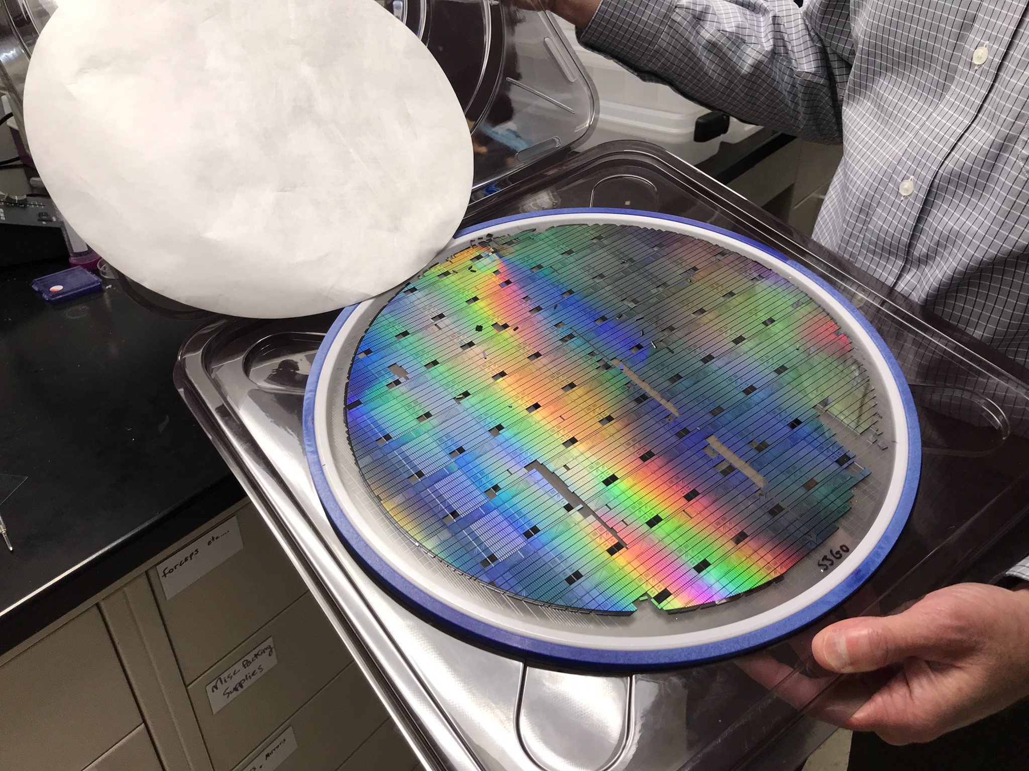
AIM has the world’s only open-access 300mm integrated photonics packaging prototyping foundry, with domestic industry now on-shoring previous overseas efforts.  The associated Test, Assembly, & Packaging (TAP) Facility in Rochester, New York is also state-of-the-art, and will be the only domestic facility of its kind, allowing export-controlled test, assembly and packaging.
 
AIM Academy
AIM Photonics Academy spearheads EWD initiatives in integrated photonics at every level of technical expertise and leads the creation of the technology roadmap that guides the $350 billion semiconductor industry in this field.